
Supplier: Shenzhen Thriver Digital Tech Co., Ltd
Address: 5F No. 535, Jihua Road, Bantian Street, Longgang Dist, Shenzhen, Guangdong
Country: China
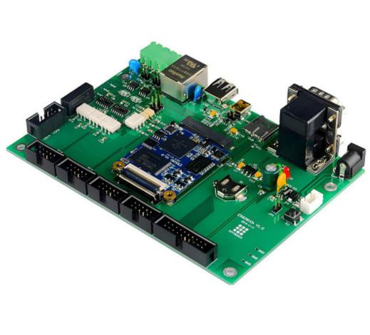
Electronic Care Device PCB Board Assembly
Price:
Pressure Sensor Medical Electronic Care Device PCB Board Assembly
Industry-specific attributes
Base Material FR4/ALU/FPC
Board Thickness 0.4MM/0.6MM/0.8MM/1MM/1.6MM
Other attributes
Model Number
Place of Origin Guangdong, China
Copper Thickness 0.5OZ/1OZ
Min. Hole Size 0.075mm
Min. Line Width 0.075mm
Min. Line Spacing 0.075mm
Surface Finishing immersion gold/ENIG/HASL
Board Size Custom
MOQ 1pcs
Service One-Stop OEM Service
Customize Avaliable
PCB Standard IPC-II Standard Shape Irregular
Package Vaccum Package
Capacity High Dirt Holding Capacity
Test service 100% E-Testing
Technics Reflow/soldering
Product name Sensor Medical PCB PCBA Circuit Board Assembly Contract Manufacturer
Thriver Digital Tech – Best Choice for PCB Electronic Board Assembly
During the process of PCB design and PCB manufacturing, our company adopts a series of systematic methods to ensure that each link can achieve high standards of quality and efficiency.
PCB Design Process
Requirement Analysis
Before the PCB electronic board assembly design begins, we first communicate with customers to understand the functional requirements, performance indicators and physical dimensions of their products. This step ensures that we can tailor the PCB design for our customers.
Schematic Design
Engineers use professional PCB design software to create a schematic diagram of the circuit to clarify the function of the circuit and the placement of components. The accuracy of the schematic is crucial for subsequent PCB manufacturing.
Layout Planning
After the schematic is completed, we carry out PCB layout planning. This includes considering factors such as signal flow, electromagnetic compatibility, thermal management, and power distribution to optimize the performance of the circuit board.
Design Rule Checking
We use automated tools to check whether the design meets specific design rules, including trace width, spacing, etc., to ensure that the design meets manufacturing and electrical specifications.
Signal and Thermal Analysis
Signal integrity analysis and thermal analysis are performed through simulation software to ensure that the PCB can work stably under high load.
Output photolithography file
Finally, we convert the design into a photolithography file, which directly affects the quality and accuracy of the subsequent photolithography process.
For more information, please visit our website.


")


CATEGORY
 Agriculture